
SP8T Absorptive RF Switch, 0.1–20 GHz ERS-0120-010
0.1–20 GHz · Absorptive SP8T · TTL control · 120 ns typical switching speed · SMA female ports
Ultra-wideband absorptive SP8T RF switch optimized for signal routing up to 20 GHz. The compact nickel-plated module provides eight routed outputs, high isolation and a three-bit TTL control interface.
Pricing and availability may change without notice.
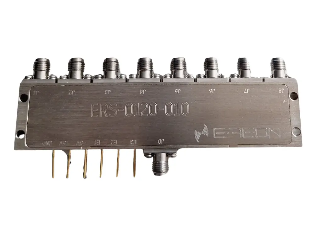
Overview
Highlights
- Ultra-wideband frequency coverage from 0.1 GHz to 20 GHz
- Absorptive SP8T topology with one common port and eight routed outputs
- 80 dB typical isolation
- 120 ns typical switching speed
- RoHS and REACH compliant
Integration notes
- Use stable TTL drive levels and do not leave control inputs floating
- Provide clean +5 V and −5 V supply rails with local decoupling
- Terminate unused RF ports with 50-ohm loads for best repeatability
- Designed for low-power cold-switching applications
Applications
- Automated Test Equipment and automated RF routing
- Radar, electronic-warfare and broadband receiver systems
- Laboratory switching matrices and RF test benches
- Multi-band communication subsystems
- RF front ends and production-line signal routing
Key specifications
| Frequency range | 0.1–20 GHz |
|---|---|
| Topology | Absorptive SP8T |
| System impedance | 50 Ω |
| Insertion loss | 4.5 dB typical, 5.0 dB maximum |
| VSWR | 1.7:1 typical, 2.0:1 maximum |
| Isolation | 80 dB typical |
| Switching speed | 120 ns typical |
| Input power | 1 W maximum |
| Control | Three-bit TTL, E3 / E2 / E1 |
| +5 V supply current | 400 mA typical |
| −5 V supply current | 50 mA typical |
| Operating temperature | −45 °C to +85 °C |
Electrical values are specified at 25 °C, sea level and with 50-ohm source and load impedances unless otherwise stated. Specifications are subject to change without notice.
Control
The common RF port J0 is routed to one of the eight output ports using the E3, E2 and E1 TTL selection lines.
TTL control interface
Apply the +5 V and −5 V supply rails within specification before changing the TTL selection inputs. Use defined logic levels and avoid slow edges or floating control inputs.
Recommended operating sequence
- Terminate unused RF ports with 50-ohm loads.
- Apply the +5 V and −5 V supply rails.
- Set E3, E2 and E1 to select the required output path.
- Apply RF at low power, then operate within the rated input-power limit.
TTL high is 2.8 V to 5.0 V. TTL low is 0 V to 0.8 V.
Truth table (E3 / E2 / E1)
0 0 0
|
Route J0 to J1 |
|---|---|
0 0 1
|
Route J0 to J2 |
0 1 0
|
Route J0 to J3 |
0 1 1
|
Route J0 to J4 |
1 0 0
|
Route J0 to J5 |
1 0 1
|
Route J0 to J6 |
1 1 0
|
Route J0 to J7 |
1 1 1
|
Route J0 to J8 |
Remove RF drive before shutdown, then place the control inputs in a defined state before removing the supply rails.
Mechanical
Construction
- 104 × 24 × 10.2 mm overall dimensions
- 65 g typical weight
- Nickel-plated housing
- Four Ø2.7 mm through mounting holes
Interfaces and handling
- One SMA female common RF port, J0
- Eight SMA female routed output ports, J1 to J8
- Control header for E3, E2, E1, −5 V, +5 V and ground
- Use ESD precautions and avoid side-loading the SMA connectors
Outline drawing
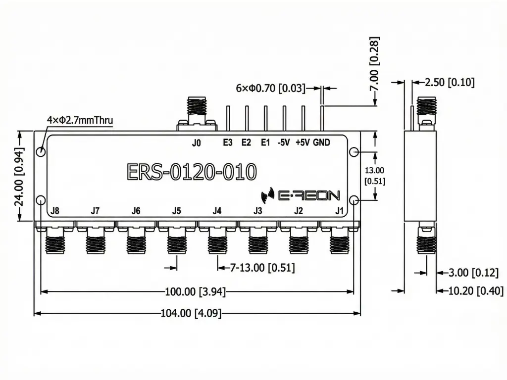
See the released datasheet for complete dimensional information and tolerances.